 2023/9/19 15:04:43
 642
642
· Choice of Memory Organizations
- SN74V263-8192 X 18/16384 X 9
- SN74V273 - 16384 x 18/32768 x 9
- SN74V283- 32768 x 18/65536 x 9
- SN74V293-65536 x 18/131072 X 9
· 166-MHz Operation
· 6-ns Read/Write Cycle Time
· UserSelectable Input and Output Port BusSizingx9 in to x9 out
- x9 in to x18 out
- x18 in to x9 out
- x18 in to x18 out
· Big-Endian/Little-Endian User-SelectableByte Representation
· 5V-Tolerant Inputs
· Fixed, Low First-Word Latency
· Zero-Latency Retransmit
· Master Reset Clears Entire FIFO
· Partial Reset Clears Data, but RetainsProgrammable Settings
· Empty, Full, and Half-Full Flags Signal FIFO Status
· Programmable Almost-Empty andAlmost-Full Flags; Each Flag Can Default toOne of Eight Preselected Offsets
· Selectable Synchronous/AsynchronousTiming Modes for Almost-Empty andAlmost-Full Flags
· Program Programmable Flags by EitherSerial or Parallel Means
· Select Standard Timing (Using EF and FFFlags) or First-Word Fall-Through (FWFTTiming (Using OR and IR Flags)
· Output Enable Puts Data Outputs inHigh-lmpedance State
· Easily Expandable in Depth and WidthIndependent Read and Write Clocks PermitReading and Writing SimultaneouslyHigh-Performance Submicron CMOSTechnology
· Glueless Interface With "C6x DSPs
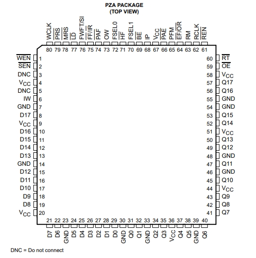
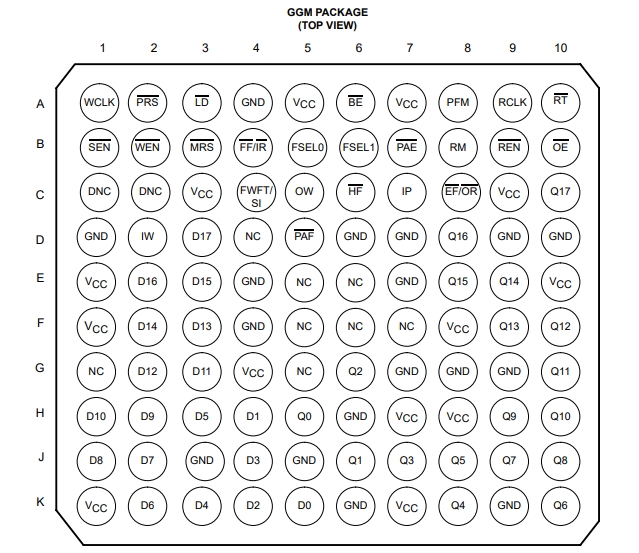
· Available in 80Pin Thin Quad Flat PackTQFP) and 100-Pin Ball Grid Array (BGA)Packages
Description
The SN74V263, SN74V273, SN74V283, and SN74V293 are exceptionally deep, high-speed, CMOS first-in first-out (FIFO) memories with clocked read and write controls and a flexible bus-matching ×9/×18 data flow.
There is flexible ×9/×18 bus matching on both read and write ports.
The period required by the retransmit operation is fixed and short.
The first-word data-latency period, from the time the first word is written to an empty FIFO to the time it can be read, is fixed and short.
These FIFOs are particularly appropriate for network, video, telecommunications, data communications, and other applications that need to buffer large amounts of data and match buses of unequal sizes.
Each FIFO has a data input port (Dn) and a data output port (Qn), both of which can assume either an 18-bit or 9-bit width, as determined by the state of external control pins input width (IW) and output width (OW) during the master-reset cycle.
The input port is controlled by write-clock (WCLK) and write-enable (WEN) inputs. Data is written into the FIFO on every rising edge of WCLK when WEN is asserted. The output port is controlled by read-clock (RCLK) and read-enable (REN) inputs. Data is read from the FIFO on every rising edge of RCLK when REN is asserted. An output-enable (OE) input is provided for 3-state control of the outputs.
热门型号
热门资讯
20万现货SKU
品类不断扩充
科技智能大仓储
4小时快速交货
仅从原厂和代理商进货
每一颗料均可原厂追溯
明码标价节省时间成本
一站式采购正品元器件


 工商网监
工商网监