 2024/5/28 10:47:11
 288
288
FEATURES
• Available in the Texas Instruments NanoFree™ Package
• Supports 5-V VCC Operation
• Inputs Accept Voltages to 5.5 V
• Max tpd of 4.7 ns at 3.3 V
• Low Power Consumption, 10-μA Max ICC
• ±24-mA Output Drive at 3.3 V
• Typical VOLP (Output Ground Bounce)<0.8 V at VCC = 3.3 V, TA = 25°C
• Typical VOHV (Output VOH Undershoot)>2 V at VCC = 3.3 V, TA = 25°C
• Ioff Supports Live Insertion, Partial-Power- Down Mode and Back Drive Protection
• Latch-Up Performance Exceeds 100 mA Per JESD 78, Class II
• ESD Protection Exceeds JESD 22
– 2000-V Human-Body Model (A114-A)
– 200-V Machine Model (A115-A)
– 1000-V Charged-Device Model (C101)
DESCRIPTION
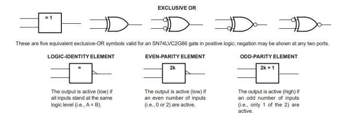
This dual 2-input exclusive-OR gate is designed for 1.65-V to 5.5-V VCC operation.
The SN74LVC2G86 performs the Boolean function Y = A ⊕ B or Y = AB AB in positive logic.
NanoFree™ package technology is a major breakthrough in IC packaging concepts, using the die as the package.
A common application is as a true/complement element. If the input is low, the other input is reproduced in true form at the output. If the input is high, the signal on the other input is reproduced inverted at the output.
This device is fully specified for partial-power-down applications using Ioff. The Ioff circuitry disables the outputs, preventing damaging current backflow through the device when it is powered down.
热门型号
热门资讯
20万现货SKU
品类不断扩充
科技智能大仓储
4小时快速交货
仅从原厂和代理商进货
每一颗料均可原厂追溯
明码标价节省时间成本
一站式采购正品元器件


 工商网监
工商网监