 2024/7/10 14:54:51
 333
333
1 Features
• Latch-Up Performance Exceeds 100 mA Per JESD 78, Class II
• ESDProtection Exceeds JESD 22
– APort
– 2500 VHuman-Body Model (A114-B)
– 200VMachine Model (A115-A)
– 1500 VCharged-Device Model (C101)
– BPort
– 8kVHuman-Body Model (A114-B)
– 200VMachine Model (A115-A)
– 1500 VCharged-Device Model (C101)
• NoDirection-Control Signal Needed
• Maximum Data Rates
– 24Mbps(Push Pull)
– 2Mbps(Open Drain)
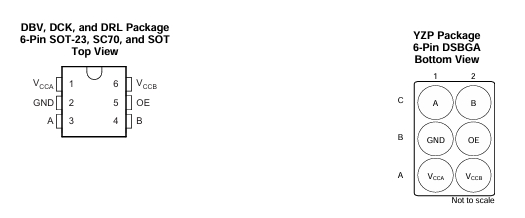
• Available in the Texas Instruments NanoFree™ Package
• 1.65 V to 3.6 V on A port and 2.3 V to 5.5 V on B port (VCCA ≤ VCCB)
• VCCIsolation Feature– If Either VCC Input Is at GND, Both Ports Are in the High-Impedance State
• NoPower-Supply Sequencing Required– Either VCCA or VCCB Can be Ramped First
• Ioff Supports Partial-Power-Down Mode Operation
2 Applications
• Handsets
• Smartphones
• Tablets
• Desktop PCs
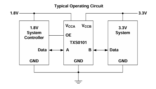
3 Description
This one-bit non-inverting translator uses two separate configurable power-supply rails. The A port is designed to track VCCA. VCCA accepts any supply voltage from 1.65 V to 3.6 V. The B port is designed to track VCCB. VCCA must be less than or equal to VCCB. VCCB accepts any supply voltage from 2.3 V to 5.5 V. This allows for low voltage bidirectional translation between any of the 1.8 V, 2.5 V, 3.3 V, and 5 V voltage nodes.
When the output-enable (OE) input is low, all outputs are placed in the high-impedance state.
To ensure the high-impedance state during power up or power down, OE should be tied to GND through a pull-down resistor; the minimum value of the resistor is determined by the current-sourcing capability of the driver.
热门型号
热门资讯
20万现货SKU
品类不断扩充
科技智能大仓储
4小时快速交货
仅从原厂和代理商进货
每一颗料均可原厂追溯
明码标价节省时间成本
一站式采购正品元器件


 工商网监
工商网监