 2024/7/19 13:59:01
 659
659
1 Features
• Available in the Ultra Small 0.64-mm2 1 Package (DPW) With 0.5-mm Pitch
• Supports 5-V VCC Operation
• Inputs Accept Voltages to 5.5 V
• Provides Down Translation to VCC
• Maxtpd of 3.7 ns at 3.3 V
• LowPower Consumption, 10-μA Max ICC
• ±24-mA Output Drive at 3.3 V
• Ioff Supports Live Insertion, Partial-Power-Down Mode, and Back-Drive Protection
• Latch-Up Performance Exceeds 100 mA Per JESD 78, Class II
• ESDProtection Exceeds JESD 22
– 2000-V Human-Body Model (A114-A)
– 200-V Machine Model (A115-A)
– 1000-V Charged-Device Model (C101)
2 Applications
• Cable Modem Termination System
• High-Speed Data Acquisition and Generation
• Military: Radar and Sonar
• Motor Control: High-Voltage
• Power Line Communication Modem
• SSD: Internal or External
• Video Broadcasting and Infrastructure: Scalable Platform
• Video Broadcasting: IP-Based Multi-Format Transcoder
• Video Communications System
3 Description
This bus buffer gate is designed for 1.65-V to 5.5-V VCC operation.
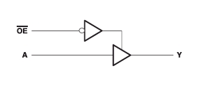
The SN74LVC1G125 device is a single line driver with a 3-state output. The output is disabled when the output-enable (OE) input is high.
The CMOS device has high output drive while maintaining low static power dissipation over a broad VCC operating range.
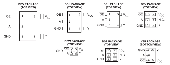
The SN74LVC1G125 device is available in a variety of packages including the ultra-small DPW package with a body size of 0.8 mm × 0.8 mm.
热门型号
热门资讯
20万现货SKU
品类不断扩充
科技智能大仓储
4小时快速交货
仅从原厂和代理商进货
每一颗料均可原厂追溯
明码标价节省时间成本
一站式采购正品元器件


 工商网监
工商网监