 2024/7/9 16:48:41
 476
476
1 Features
• Latch-up performance exceeds 100 mA Per JESD 78, Class II
• ESDprotection exceeds JESD 22
– 2000-V Human-body model (A114-A)
– 200-V Machine model (A115-A)
– 1000-V Charged-device model (C101)
• Available in the Texas Instruments NanoStar™ and NanoFree™ Packages
• Supports 5-V VCC operation
• Inputs accept voltages to 5.5 V
• Supports down translation to VCC
• Maximum tpd of 4.5 ns at 3.3 V
• Lowpower consumption, 10-µA maximum ICC
• ±24-mA Output drive at 3.3 V
• Ioff Supports partial-power-down mode and back drive protection
2 Applications
• AVreceivers
• Blu-ray players and home theaters
• DVDrecorders and players
• Desktop or notebook PCs
• Digital radio or internet radio players
• Digital video cameras (DVC)
• Embedded PCs
• GPS:personal navigation devices
• Mobile internet devices
• Network projector front-ends
• Portable media players
• Proaudio mixers
• Smokedetectors
• Solid dtate drive (SSD): enterprise
• High-definition (HDTV)
• Tablets: enterprise
• Audio docks: portable
• DLPfront projection systems
• DVRandDVS
• Digital picture frame (DPF)
• Digital still cameras

3 Description
The SN74LVC1G38 device is designed for 1.65-V to 5.5-V VCC operation.
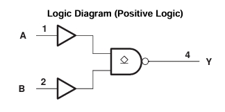
This device is a single two-input NAND buffer gate with open-drain output. It performs the Boolean function Y = A × B or Y = A B in positive logic.
This device is fully specified for partial-power-down applications using Ioff. The Ioff circuitry disables the outputs when the device is powered down. This inhibits current backflow into the device which prevents damage to the device.
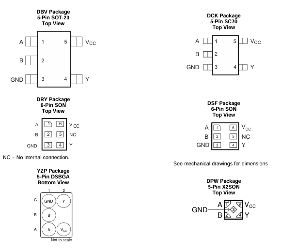
NanoStar™ and NanoFree™ package technology is a major breakthrough in IC packaging concepts, using the die as the package.

热门型号
热门资讯
20万现货SKU
品类不断扩充
科技智能大仓储
4小时快速交货
仅从原厂和代理商进货
每一颗料均可原厂追溯
明码标价节省时间成本
一站式采购正品元器件