 2024/4/10 16:38:05
 177
177
FEATURES
• Operates From 1.65 V to 3.6 V
• Max t pd of 3.3 ns at 3.3 V
• ±24-mA Output Drive at 3.3 V
• Bus Hold on Data Inputs Eliminates the Need for External Pullup/Pulldown Resistors
• Latch-Up Performance Exceeds 100 mA Per JESD 78, Class II
• ESD Protection Exceeds JESD 22
– 2000-V Human-Body Model (A114-A)
– 200-V Machine Model (A115-A)
– 1000-V Charged-Device Model (C101)
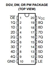
DESCRIPTION/ORDERING INFORMATION
This octal transparent D-type latch is designed for 1.65-V to 3.6-V VCC operation.
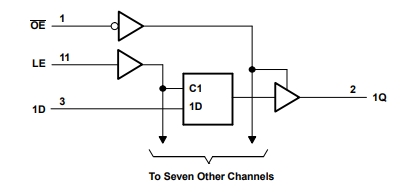
The SN74ALVCH373 is particularly suitable for implementing buffer registers, I/O ports, bidirectional bus drivers, and working registers. While the latch-enable (LE) input is high, the Q outputs follow the data (D) inputs. When LE is taken low, the Q outputs are latched at the logic levels set up at the D inputs.
A buffered output-enable (OE) input can be used to place the eight outputs in either a normal logic state (high or low logic levels) or the high-impedance state. In the high-impedance state, the outputs neither load nor drive the bus lines significantly. The high-impedance state and increased drive provide the capability to drive bus lines without interface or pullup components.
OE does not affect the internal operations of the latches. Old data can be retained or new data can be entered while the outputs are in the high-impedance state.
To ensure the high-impedance state during power up or power down, OE should be tied to VCC through a pullup resistor; the minimum value of the resistor is determined by the current-sinking capability of the driver.
Active bus-hold circuitry holds unused or undriven inputs at a valid logic state. Use of pullup or pulldown resistors with the bus-hold circuitry is not recommended.
热门型号
热门资讯
20万现货SKU
品类不断扩充
科技智能大仓储
4小时快速交货
仅从原厂和代理商进货
每一颗料均可原厂追溯
明码标价节省时间成本
一站式采购正品元器件


 工商网监
工商网监