 2023/10/19 16:23:32
 222
222
FEATURES
? Single 1.8V Power Supply Operation.
? Power Scaling with Clock Frequency.
? Internal Sample-and-Hold.
? Internal or External Reference.
? Power Down Mode.
? Offset Binary or 2 s Complement Output Data Format.
? LVDS or CMOS Output Signals.
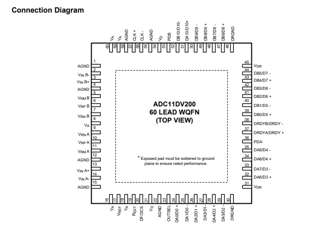
? 60-Pin WQFN Package, (9x9x0.8mm, 0.5mm Pin-Pitch)
? Clock Duty Cycle Stabilizer.
? IF Sampling Bandwidth > 900MHz.
APPLICATIONS
? Digital Predistortion (DPD)
? Wireless Communications Infrastructure
? Medical Imaging
? Portable Instrumentation
? Digital Video
KEY SPECIFICATIONS
? Resolution: 11 Bits
? Conversion Rate: 200 MSPS
? ENOB: 10.06 bits (typ) @Fin=70 MHz
? SNR: 62.5 dBFS (typ) @Fin=70 MHz
? SINAD: 62.3 dBFS (typ) @Fin=70 MHz
? SFDR: 82 dBFS (typ) @Fin=70 MHz
? LVDS: Power 450 mW (typ) @Fs=200 MSPS
? CMOS: Power 280 mW (typ) @Fs=170 MSPS
? Operating Temp. Range: ?40°C to 85°C.

DESCRIPTION
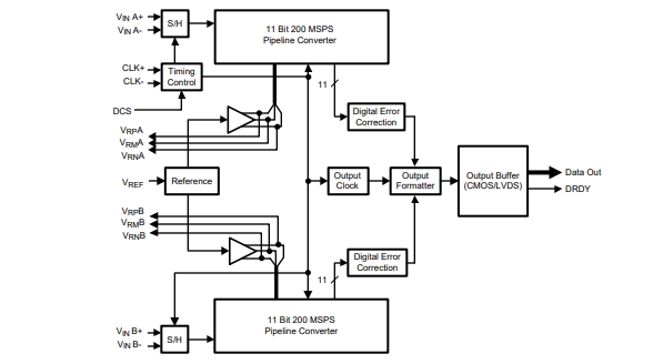
The ADC11DV200 is a monolithic analog-to-digital converter capable of converting two analog input signals into 11-bit digital words at rates up to 200 Mega Samples Per Second (MSPS). The digital output mode is selectable and can be either differential LVDS or CMOS signals. This converter uses a differential, pipelined architecture with digital error correction and an on-chip sample-and-hold circuit to minimize die size and power consumption while providing excellent dynamic performance. A unique sample-and-hold stage yields a full-power bandwidth of 900MHz. Fabricated in core CMOS process, the ADC11DV200 may be operated from a single 1.8V power supply. The ADC11DV200 achieves approximately 10.06 effective bits at Nyquist and consumes just 280mW at 170MSPS in CMOS mode 450mW at 200MSPS in LVDS mode. The power consumption can be scaled down further by reducing sampling rates.

热门型号
热门资讯
20万现货SKU
品类不断扩充
科技智能大仓储
4小时快速交货
仅从原厂和代理商进货
每一颗料均可原厂追溯
明码标价节省时间成本
一站式采购正品元器件