 2024/7/19 11:53:52
 378
378
FEATURES
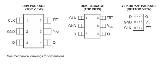
• Available in the Texas Instruments NanoStar™ and NanoFree™ Packages
• Supports 5-V VCC Operation
• Inputs Accept Voltages to 5.5 V
• Provides Down Translation to VCC
• Maxtpd of 4 ns at 3.3 V
• LowPowerConsumption, 10-μA Max ICC
• ±24-mA Output Drive at 3.3 V
• Ioff Supports Live Insertion, Partial-Power-Down Mode, and Back Drive Protection
• Latch-Up Performance Exceeds 100 mA Per JESD 78, Class II
• ESDProtection Exceeds JESD 22
– 2000-V Human-Body Model (A114-A)
– 200-V Machine Model (A115-A)
– 1000-V Charged-Device Model (C101)
DESCRIPTION
This single D-type latch is designed for 1.65-V to 5.5 V VCC operation.
The SN74LVC1G374 features a 3-state output designed specifically for driving highly capacitive or relatively low-impedance loads. This device is particularly suitable for implementing buffer registers, input/output (I/O) ports, bidirectional bus drivers, and working registers.
NanoStar™ and NanoFree™ package technology is a major breakthrough in IC packaging concepts, using the die as the package.
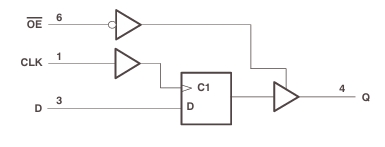
A buffered output-enable (OE) input can be used to place the output in either a normal logic state (high or low logic levels) or the high-impedance state. In the high-impedance state, the output neither loads nor drives the bus lines significantly. The high-impedance state and increased drive provide the capability to drive bus lines without interface or pullup components.
OEdoesnotaffect theinternaloperations of the flip-flop. Old data can be retained or new data can be entered while the outputs are in the high-impedance state.
To ensure the high-impedance state during power up or power down, OE should be tied to VCC through a pullup resistor; the minimum value of the resistor is determined by the current-sinking capability of the driver.
This device is fully specified for partial-power-down applications using Ioff. The Ioff circuitry disables the outputs, preventing damaging current backflow through the device when it is powered down.
热门型号
热门资讯
20万现货SKU
品类不断扩充
科技智能大仓储
4小时快速交货
仅从原厂和代理商进货
每一颗料均可原厂追溯
明码标价节省时间成本
一站式采购正品元器件


 工商网监
工商网监