 2024/7/3 14:30:31
 333
333
1 Features
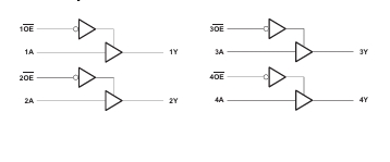
• 3-State Outputs
• Separate OE for all 4 buffers
• Operates From 1.65 V to 3.6 V
• Specified From–40°C to 85°C and–40°C to 125°C
• Inputs Accept Voltages to 5.5 V
• Maxtpd of 4.8 ns at 3.3 V
• Typical VOLP (Output Ground Bounce) < 0.8 V at VCC = 3.3 V, TA = 25°C
• Typical VOHV (Output VOH Undershoot) > 2 Vat VCC = 3.3 V, TA = 25°C
• Latch-Up Performance Exceeds 250 mA Per JESD 17
• ESDProtection Exceeds JESD 22
– 2000-V Human-Body Model
– 200-V Machine Model
– 1000-V Charged-Device Model
2 Applications
• Cable Modem Termination Systems
• IPPhones: Wired and Wireless
• Optical Modules
• Optical Networking:
– EPONorVideo Over Fiber
• Point-to-Point Microwave Backhaul
• Power: Telecom DC/DC Modules:
– Analog or Digital
• Private Branch Exchanges (PBX)
• TETRABase Stations
• Telecom Base Band Units
• Telecom Shelters:
– Filter Unit s
– Power Distribution Units (PDU)
– Power Monitoring Units (PMU)
– Wireless Battery Monitoring
– Remote Electrical Tilt Units (RET)
– Remote Radio Units (RRU)
– Tower Mounted Amplifiers (TMA)
• Vector Signal Analyzers and Generators
• Video Conferencing: IP-Based HD
• WiMAXandWireless Infrastructure Equipment
• Wireless Communications Testers
• xDSLModems and DSLAM
3 Description
This quadruple bus buffer gate is designed for 1.65-V to 3.6-V VCC operation.
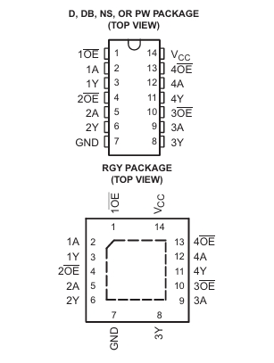
The SN74LVC125A device features independent line drivers with 3-state outputs. Each output is disabled when the associated output-enable (OE) input is high.
To ensure the high-impedance state during power up or power down, OE should be tied to VCC through a pullup resistor; the minimum value of the resistor is determined by the current-sinking capability of the driver.
Inputs can be driven from either 3.3-V or 5-V devices. This feature allows the use of this device as a translator in a mixed 3.3-V/5-V system environment.
热门型号
热门资讯
20万现货SKU
品类不断扩充
科技智能大仓储
4小时快速交货
仅从原厂和代理商进货
每一颗料均可原厂追溯
明码标价节省时间成本
一站式采购正品元器件


 工商网监
工商网监