 2024/7/5 13:49:24
 322
322
· Inputs Are TTL-Voltage Compatible
· Latch-Up Performance Exceeds 250 mA Per JESD 17
· ESD Protection Exceeds JESD 22
– 2000-V Human-Body Model (A114-A)
– 200-V Machine Model (A115-A)
– 1000-V Charged-Device Model (C101)
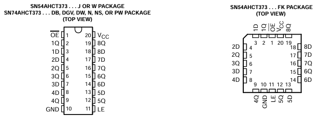
description/ordering information
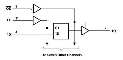
The ’AHCT373 devices are octal-transparent D-type latches. When the latch-enable (LE) input is high, the Q outputs follow the data (D) inputs. When LE is low, the Q outputs are latched at the logic levels of the D inputs.
A buffered output-enable (OE) input can be used to place the eight outputs in either a normal logic state (high or low) or the high-impedance state. In the high-impedance state, the outputs neither load nor drive the bus lines significantly. The high-impedancestate and increased drive provide the capability to drive bus lines without interface or pullup components.
OE does not affect the internal operations of the latches. Old data can be retained or new data can be entered while the outputs are in the high-impedance state.
To ensure the high-impedance state during power up or power down, OE should be tied to VCC through a pullup resistor; the minimum value of the resistor is determined by the current-sinking capability of the driver.
热门型号
热门资讯
20万现货SKU
品类不断扩充
科技智能大仓储
4小时快速交货
仅从原厂和代理商进货
每一颗料均可原厂追溯
明码标价节省时间成本
一站式采购正品元器件


 工商网监
工商网监