 2024/7/3 11:47:50
 68
68
1 Features
• Operating Range 2-V to 5.5-V VCC 1
• Contain Eight Flip-Flops With Single-Rail Outputs
• Direct Clear Input
• Individual Data Input to Each Flip-Flop
• Latch-Up Performance Exceeds 250 mA Per JESD 17
• ESDProtection Exceeds JESD 22
– 2000-V Human-Body Model (A114-A)
– 1000-V Charged-Device Model (C101)
• OnProducts Compliant to MIL-PRF-38535, All Parameters Are Tested Unless Otherwise Noted. On All Other Products, Production Processing Does Not Necessarily Include Testing of All Parameters.
2 Applications
• Buffers and Storage Registers
• Shift Registers
• Pattern Generators
• Servers
• PCsandNotebooks
• Network Switches
• Memory Systems
• Databases
3 Description
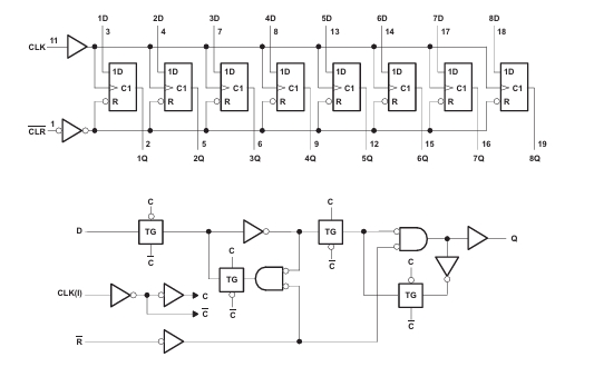
These devices are positive-edge-triggered D-type flip-flops with a direct clear (CLR) input.
Information at the data (D) inputs meeting the setup time requirements is transferred to the Q outputs on the positive-going edge of the clock (CLK) pulse. Clock triggering occurs at a particular voltage level and is not directly related to the transition time of the positive-going pulse. When CLK is at either the high or low level, the D input has no effect at the output.
热门型号
热门资讯
20万现货SKU
品类不断扩充
科技智能大仓储
4小时快速交货
仅从原厂和代理商进货
每一颗料均可原厂追溯
明码标价节省时间成本
一站式采购正品元器件


 工商网监
工商网监