 2024/7/9 15:51:41
 368
368
Features
• Buffered Inputs
• Four Operating Modes: Shift Left, Shift Right, Load and Store
• Can be Cascaded for N-Bit Word Lengths
• I/O0 - I/O7 Bus Drive Capability and Three-State for Bus Oriented Applications
• Typical fMAX = 50MHz at VCC =5V,CL=15pF, TA=25oC
• Fanout (Over Temperature Range)
- Standard Outputs. . . . . . . . . . . . . . . 10 LSTTL Loads
- Bus Driver Outputs . . . . . . . . . . . . . 15 LSTTL Loads
• Wide Operating Temperature Range . . .-55oC to 125oC
• Balanced Propagation Delay and Transition Times
• Significant Power Reduction Compared to LSTTL Logic ICs
• HC Types
- 2V to 6V Operation
- High Noise Immunity: NIL = 30%, NIH = 30% of VCC at VCC = 5V
• HCT Types- 4.5V to 5.5V Operation
- Direct LSTTL Input Logic Compatibility, VIL= 0.8V (Max), VIH = 2V (Min)
- CMOS Input Compatibility, Il ≤ 1µA at VOL, VOH
Description
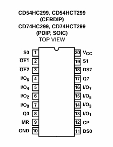
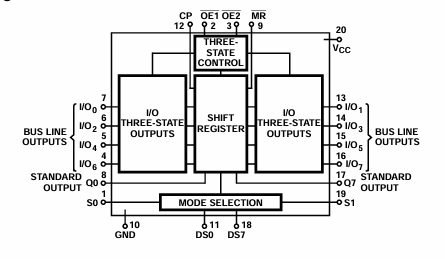
The ’HC259 and ’HCT299 are 8-bit shift/storage registers with three-state bus interface capability. The register has four synchronous-operating modes controlled by the two select inputs as shown in the mode select (S0, S1) table. The mode select, the serial data (DS0, DS7) and the parallel data (I/O0- I/O7) respond only to the low-to-high transition of the clock (CP) pulse. S0, S1 and data inputs must be stable one set up time prior to the clock positive transition.
The Master Reset (MR) is an asynchronous active low input. When MR output is low, the register is cleared regardless of the status of all other inputs. The register can be expanded by cascading same units by tying the serial output (Q0) to the serial data (DS7) input of the preceding register, and tying the serial output (Q7) to the serial data (DS0) input of the following register. Recirculating the (n x 8) bits is accomplished by tying the Q7 of the last stage to the DS0 of the first stage.
The three-state input/output I(/O) port has three modes of operation:
1. Bothoutputenable(OE1andOE2)inputsarelowandS0 or S1 or both are low, the data in the register is presented at the eight outputs.
2. Whenboth S0 and S1are high, I/O terminals are in the high impedance state but being input ports, ready for par allel data to be loaded into eight registers with one clock transition regardless of the status of OE1 and OE2.
3. Either one of the two output enable inputs being high will force I/O terminals to be in the off-state. It is noted that each I/O terminal is a three-state output and a CMOS buffer input.
热门型号
热门资讯
20万现货SKU
品类不断扩充
科技智能大仓储
4小时快速交货
仅从原厂和代理商进货
每一颗料均可原厂追溯
明码标价节省时间成本
一站式采购正品元器件


 工商网监
工商网监