 2024/4/16 16:32:19
 27
27
1 Features
• ESD Protection Exceeds JESD 22
– 2000-V Human-Body Model (A114-A)
– 200-V Machine Model (A115-A)
– 1000-V Charged-Device Model (C101)
• Available in the Texas Instruments NanoFree™ Package
• Fully Configurable Dual-Rail Design Allows Each Port to Operate Over the Full 1.65-V to 5.5-V Power-Supply Range
• VCC Isolation Feature
– If Either VCC Input Is at GND, Both Ports Are in the High-Impedance State
• DIR Input Circuit Referenced to VCCA
• Low Power Consumption, 4-µA Max ICC
• ±24-mA Output Drive at 3.3 V
• Ioff Supports Partial-Power-Down Mode Operation
• Max Data Rates
– 420 Mbps (3.3-V to 5-V Translation)
– 210 Mbps (Translate to 3.3 V)
– 140 Mbps (Translate to 2.5 V)
– 75 Mbps (Translate to 1.8 V)
• Latch-Up Performance Exceeds 100 mA Per JESD 78, Class II
2 Applications
• Personal Electronic
• Industrial
• Enterprise
• Telecom

3 Description
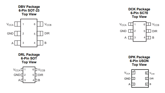
This single-bit noninverting bus transceiver uses two separate configurable power-supply rails. The A port is designed to track VCCA. VCCA accepts any supply voltage from 1.65 V to 5.5 V. The B port is designed to track VCCB. VCCB accepts any supply voltage from 1.65 V to 5.5 V. This allows for universal low-voltage bidirectional translation between any of the 1.8-V, 2.5-V, 3.3-V, and 5-V voltage nodes.
The SN74LVC1T45 is designed for asynchronous communication between two data buses. The logic levels of the direction-control (DIR) input activate either the B-port outputs or the A-port outputs. The device transmits data from the A bus to the B bus when the B-port outputs are activated and from the B bus to the A bus when the A-port outputs are activated. The input circuitry is always active on both A and B ports and must have a logic HIGH or LOW level applied to prevent excess ICC and ICCZ.
热门型号
热门资讯
20万现货SKU
品类不断扩充
科技智能大仓储
4小时快速交货
仅从原厂和代理商进货
每一颗料均可原厂追溯
明码标价节省时间成本
一站式采购正品元器件


 工商网监
工商网监