 2024/3/28 19:10:11
 36
36
1 Features
• Wide Operating Voltage Range of 2 V to 6 V
• Outputs Can Drive Up to 10 LSTTL Loads
• Low Power Consumption, 80-μA Maximum ICC
• Typical tpd = 20 ns
• ±4-mA Output Drive at 5 V
• Low Input Current of 1-μA Maximum
• AND-Gated (Enable/Disable) Serial Inputs
• Fully Buffered Clock and Serial Inputs
• Direct Clear
• On Products Compliant to MIL-PRF-38535,All Parameters Are Tested Unless Otherwise Noted. On All Other Products, Production Processing Does Not Necessarily Include Testing of All Parameters.
2 Applications
• Programable Logic Controllers
• Appliances
• Video Display Systems
• Output Expander
3 Description
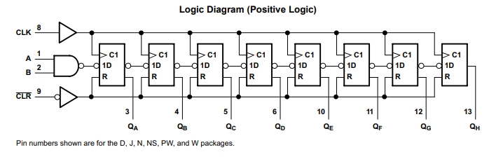
These 8-bit shift registers feature AND-gated serial inputs and an asynchronous clear (CLR) input. The gated serial (A and B) inputs permit complete control over incoming data; a low at either input inhibits entry of the new data and resets the first flip-flop to the low level at the next clock (CLK) pulse. A high-level input enables the other input, which then determines the state of the first flip-flop. Data at the serial inputs can be changed while CLK is high or low, provided the minimum set-up time requirements are met. Clocking occurs on the low-to-high-level transition of CLK.

热门型号
热门资讯
20万现货SKU
品类不断扩充
科技智能大仓储
4小时快速交货
仅从原厂和代理商进货
每一颗料均可原厂追溯
明码标价节省时间成本
一站式采购正品元器件


 工商网监
工商网监