 2024/3/27 16:18:10
 30
30
FEATURES
• Available in the Texas Instruments NanoStar™ Packages
• Single-Supply Voltage Translator
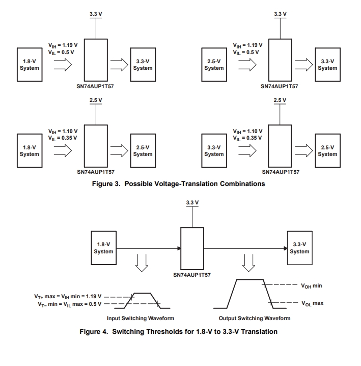
• 1.8 V to 3.3 V (at VCC = 3.3 V)
• 2.5 V to 3.3 V (at VCC = 3.3 V)
• 1.8 V to 2.5 V (at VCC = 2.5 V)
• 3.3 V to 2.5 V (at VCC = 2.5 V)
• Nine Configurable Gate Logic Functions
• Schmitt-Trigger Inputs Reject Input Noise and Provide Better Output Signal Integrity
• Ioff Supports Partial-Power-Down Mode With Low Leakage Current (0.5 mA)
• Very Low Static and Dynamic Power Consumption
• Pb-Free Packages Available: SON (DRY or DSF), SOT-23 (DBV), SC-70 (DCK), and NanoStar WCSP
• Latch-Up Performance Exceeds 100 mA Per JESD 78, Class II
• ESD Performance Tested Per JESD 22
– 2000-V Human-Body Model (A114-B, Class II)
– 1000-V Charged-Device Model (C101)
• Related Devices: SN74AUP1T58, SN74AUP1T97, and SN74AUP1T98

DESCRIPTION/ORDERING INFORMATION
AUP technology is the industry s lowest-power logic technology designed for use in battery-operated or battery backed-up equipment. The SN74AUP1T57 is designed for logic-level translation applications with input switching levels that accept 1.8-V LVCMOS signals, while operating from either a single 3.3-V or 2.5-V VCC supply.
The wide VCC range of 2.3 V to 3.6 V allows the possibility of battery voltage drop during system operation and ensures normal operation between this range.
Schmitt-trigger inputs (ΔVT = 210 mV between positive and negative input transitions) offer improved noise immunity during switching transitions, which is especially useful on analog mixed-mode designs. Schmitt-trigger inputs reject input noise, ensure integrity of output signals, and allow for slow input signal transition.
The SN74AUP1T57 can be easily configured to perform a required gate function by connecting A, B, and C inputs to VCC or ground (see Function Selection table). Up to nine commonly used logic gate functions can be performed.
Ioff is a feature that allows for powered-down conditions (VCC = 0 V) and is important in portable and mobile applications. When VCC = 0 V, signals in the range from 0 V to 3.6 V can be applied to the inputs and outputs of the device. No damage occurs to the device under these conditions.
The SN74AUP1T57 is designed with optimized current-drive capability of 4 mA to reduce line reflections, overshoot, and undershoot caused by high-drive outputs.
NanoStar package technology is a major breakthrough in IC packaging concepts, using the die as the package.
热门型号
热门资讯
20万现货SKU
品类不断扩充
科技智能大仓储
4小时快速交货
仅从原厂和代理商进货
每一颗料均可原厂追溯
明码标价节省时间成本
一站式采购正品元器件


 工商网监
工商网监