 2024/1/5 14:20:14
 243
243
1 Features
• Wide Range of Digital and Analog Signal Levels
– Digital: 3 V to 20 V
– Analog: ≤ 20 VP-P
• Low ON Resistance, 125 Ω (Typical) Over 15 VP-P Signal Input Range for VDD – VEE = 18 V
• High OFF Resistance, Channel Leakage of ±100 pA (Typical) at VDD – VEE = 18 V
• Logic-Level Conversion for Digital Addressing Signals of 3 V to 20 V (VDD – VSS = 3 V to 20 V) to Switch Analog Signals to 20 VP-P (VDD – VEE = 20 V) Matched Switch Characteristics, rON = 5 Ω (Typical) for VDD – VEE = 15 V Very Low Quiescent Power Dissipation Under All Digital-Control Input and Supply Conditions, 0.2 µW (Typical) at VDD – VSS = VDD – VEE = 10 V
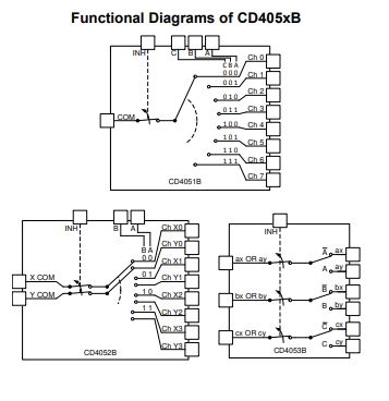
• Binary Address Decoding on Chip
• 5 V, 10 V, and 15 V Parametric Ratings
• 100% Tested for Quiescent Current at 20 V
• Maximum Input Current of 1 µA at 18 V Over Full Package Temperature Range, 100 nA at 18 V and 25°C
• Break-Before-Make Switching Eliminates Channel Overlap
2 Applications
• Analog and Digital Multiplexing and Demultiplexing
• A/D and D/A Conversion
• Signal Gating
• Factory Automation
• Televisions
• Appliances
• Consumer Audio
• Programmable Logic Circuits
• Sensors
3 Description
The CD405xB analog multiplexers and demultiplexers are digitally-controlled analog switches having low ON impedance and very low OFF leakage current. These multiplexer circuits dissipate extremely low quiescent power over the full VDD – VSS and VDD – VEE supply-voltage ranges, independent of the logic state of the control signals.
热门型号
热门资讯
20万现货SKU
品类不断扩充
科技智能大仓储
4小时快速交货
仅从原厂和代理商进货
每一颗料均可原厂追溯
明码标价节省时间成本
一站式采购正品元器件


 工商网监
工商网监